The Facinating Quantum World of Two-dimensional Materials
Jun 05, 2021My name is Katrina Cole Anderson, I am the Dean of Research at the Technical University of Denmark and I would like to welcome everyone to this lecture on HCl today by our guest visitor from UC Berkeley, Stephen Lewis. We are very happy to have you sitting today in this view and I would also like to welcome all of our visitors, our guests, our students, colleagues, everyone who is here today for this Earth Day conference, as the conferences have been held at a TCU location for approximately 20 years and It is an opportunity for us to invite you all to talks by some of the
world
's leading scientists on fascinating and inspiring topics from their research and make us aware of what is happening out there and hopefully inspire some of you students, but also some.
The American scientists who work to teach you and see what is happening in places other than our University and hopefully also to build or strengthen collaborations for the future, these conferences are called HTS conferences and yes, you probably still know it. He was the founder of our university in 1829 and in 2020 we were going to celebrate that it is the 200th anniversary of his invention or his discovery of electromagnetism and for that reason we are also preparing for this event in 2020 and we will focus more on that in the next conferences in general we will have another two conferences per year this year, actually we have three, so the next one will be on December 4th and you may already want to put that as a highlight. that's on your schedule so you're ready to be here again for the next lecture, but I think with that I'll turn the
world
over to a casting professor, Kyle Larson, from TCU physics, who will give you a further introduction to Steven Louie and This is a talk today called The Fascinating Quantum World of Two-Dimensional Materials and I'm looking forward to learning more about it.
More Interesting Facts About,
the facinating quantum world of two dimensional materials...
Thank you, ladies and gentlemen, Professor Louie. It is a great pleasure and honor to introduce Professor Stephen Louis as today's austere lecturer. Steve Louie received his PhD in physics from the University of California at Berkeley in 1976, then worked at IBM's Watson Research Center Bell Labs and the University of Penn, then returned to UC Berkeley in 1980, where he is now a professor of physics and At the same time, he is a senior faculty scientist at Lawrence Berkeley National Laboratory. Steve Lewis is an elected member of the National Academy of Sciences and the American Academy of Arts and Sciences.

He is a member of the American Physical Society and the American Association for the Advancement of Science. He has received numerous awards and recognitions and to mention a few of them, he received the APS and SRA Raman Award for Computational Physics, the APS Davidson Germer Price and Surface Physics, the Self Research Society War Materials Theory and also the Provident Institute that had the Fineman price. in nanotechnology, he is also a professor of DubLi at Chalmers University, near here. Stephen Lewis's research lies within the field of theoretical condensed matter physics and nanoscience. To put his work in a historical context, the basic theory behind his work, namely
quantum
mechanics, was born around a hundred years ago, at first the new theory focused mainly on atoms and molecules, but during the In the last century,quantum
mechanics has gradually made its way toward understanding condensed matter systems andmaterials
, much of which is the basic understanding of how electrons behave and behave.
The way they control material properties, including for example superconductivity, was developed around 1960 or in the 1960s. I can mention it here because we are in the Nordic countries and some of the fundamental contributions to this development were performed by several suites, including the city of Los Angeles in Steve Twist. and Bank Lundqvist and his work led to the rather peculiar term called Swedish electron gas. The last few decades have seen two dramatic changes in condensed matter and
materials
physics, probably more, but I just mentioned two. The first is the ability to control and control experimentally. investigating matter at the nanoscale leading to the new field of nanotechnology, the other change and this is where Steve Lewis's work also comes into play is the incredible increase in computational power, which means that today quantum mechanics does not It is not only a beautiful theory but also an accurate tool for understanding and predicting the properties of real materials and nanostructures.Steve Lui has been one of the leaders in developing computational methods for calculating the properties of real materials and nanostructures directly based on the Quantum mechanics, if you like, took the Swedish electron gas of the 60s and turned it into a theory and a computational approach applicable to real materials. His many contributions include the development of new computational methods for calculating electronic excitations in semiconductors on surfaces and in nanostructures. His main interest in the last decade has been low
dimensional
systems where he has pioneered the quantitative understanding of graphene and other two-dimensional
materials. If he likes some numbers, his impact has been tremendous.He has more than 60,000 quotes and the H-index of him is around 100, so with these words he is a great pleasure. Later I will give the floor to Steve Louis so that he can enlighten us in this conference on two-dimensional materials. So please, thank you very much Professor Jacobsen and Professor Anderson for the kind introduction. I feel very honored and pleased to give today's lecture. Of course, I would also like to thank the selection committee for granting me this honor. What I would like to do. In fact, I was very honored by the lists of former speakers in this lecture series, so what I would like to do today is basically I say let's share with you some of the recent work that we have done in the area of atomic sheets in two-dimensional materials.
As everyone knows, materials have played such an important role in the development of humanity that we use them to label major areas. of human history, so this is a figure I stole from the materials department website of the loud or beloved World University in the UK. So, from the Stone Age millions of years ago to the machine age of the Industrial Revolution, today, of course, Professor Hans Christian ørsted was a giant in science and also in technology and his contributions are many, including, as mentioned, the discovery that electric currents can generate magnetic fields and also the discovery of aluminum insulation and its contribution, of course.
As they certainly were essential elements for the industrial revolution than the machine age, today we are talking about the age of plastic, the age of silicon, perhaps in the ages of nanomaterials now in terms of nanomaterials, when we talk about what is the nanomaterial of man, basically we are talking about material with structure. that's at least nanoscale and dimension along one of the directions, so you have zero dimension nanomaterials like nanoparticle clusters, quantum dots, 1D materials like carbon nanotubes and nanowires, nanorods and then you have 2D materials including the Wells quantum semiconductor graphene and the so-called atomic sheet. int 2d materials, so this will be the topic I focus on in today's lecture, so an atomic friend of the material has been a very exciting development in the last decade and many new sciences and possible applications are emerging in this field and The best-known example of this class of material is graphene, which is basically a single layer of graphite.
Of course, there are many layers of materials in nature and they could also, and many experiments have been done, exactly, they are taking said material and making it. atomic: one or two layers, so here I saw a number of examples of this class of so-called dichotomized transition metal systems that, unlike graphene, can be semiconducting metals, even superconducting ones, so that they greatly expand the property of the 2D material that goes beyond graphene and you If you have a great insulator like boron nitride, our insulin is another class A layer material that is superconducting in the book, but if you make a single layer of this and put it on top of a substrate like strontium titanate, then you could increase this transition temperature by an order of magnitude. from about 10 degrees to a hundred degrees and you can also have 2D material that becomes a ferromagnet given that low dimension, so today I have to talk about something about this system and of course there are many researchers working in this area of air Now, as I mentioned.
There is a lot of excitement and a lot of other advances in the field, in fact, I will do at this university BTU, so in addition to looking at individual layer materials because these are materials that interact weakly perpendicular to the direction of the plane that one could Imagine doing a combination of this. The material just by stacking them and getting materials had very different properties, so that's the dream in this field. In fact, there have been some examples of this type of application in various laboratories, so in this talk I will mainly talk about the transport and the optical property of 2D systems.
Due to their restricted geometry, the property of this type of material is very influenced by quantum confinement it enhances the electron-electron interaction and Reda mentions that it reduces the effects of dimensionality and symmetry and this type of effect often leads to new properties of the phenomenon that generally do not exist in the book and are also often useful in applications in Particularly because you are talking about atomic sheet tip systems, their properties can be tuned and controlled by gates and environmental sensing, as you will see later, so this is basically In the summary of my talk, I will start with some basic concepts related to physics of the solid state because I'm told this is a pretty broad audience and then I'll talk about the additional physics or the quasi-two-dimensional crystal and then I'll move on to talk about graphene nanoribbons. which turn out to be very interesting topological electronic materials and discuss a new set of selection rules for optical transitions and 2D materials, then they talk about magnetism in 2D, how we could control it and finally, if I have time, which I may not have, it is to talk about some strange electron transport to the direct fermion system in the presence of disorder, so let me start with some very basic physics regarding solid state crystals.
I just apologize to the experts in the audience, this is basically what they learn first. year of solid state physics, the first thing I would like to mention, which I would use often is the so-called black theorem. Felix Bloch showed, after normal quantum mechanics, that for a periodic crystal, due to crystal periodicity, the electronic states in a crystal are actually extended propagation states, you could write its wave function this way where you have a vector of K and you wave is a periodic function that looks exactly the same in every unit cell and then the energy of the electronic state can be labeled by a quantum number.
K is the wave vector and some other quantum number n, so you end up having a band structure similar to what you had as K. Another thing that could be deduced from crystal symmetry is that different physical states can access only in a finite region of k. space and that's called the Breann zone, which I'll use later and the brilliant song, in fact, is a compact geometric manifold, so in one dimension it's a circle, in two dimensions it's a torus and then in three dimensions it's a higher dimension. Another challenge to understanding the condensed matter system is that you really have a system of many interacting electrons, so for many properties it is necessary to use some theoretical many-body techniques that Professor Jerison has mentioned regarding the Swedish electron gas and it turns out that today madhuri correlated electron system that could actually solve this problem numerically from the first principle using many bodies for Bayesian theory, so now let me move on to the quasi system that will be, we will look at the spectroscopic and transformed poverty probabilities. such systems, so I would like to emphasize or remind you two things from the beginning: one is that there are enhanced Coulomb interactions in such systems because in a restricted dimension the electrons cannot avoid each other as much and the second thing, which is less known is which could have a very strange and strongly dependent space screen between interacting particles in such a system and I will illustrate it through this cartoon here, suppose this year your two-dimensional crystal has two charges, I say an electron and a hole here. and interact with theCoulomb interaction Now, when the two particles are very close to each other, then the particle that is in the middle can't really shield the Coulomb interaction, so there is very weak detection, but when the two particles are further away, that electron creates a screen. the Coulomb interaction, so you would expect the shielding to increase as a function of a distant material and in the 3D vault that would quickly saturate to a constant shielding, for example, for a semiconductor, but in this type of 2D system you see that the Coulomb line We actually come out of the sample because we live in a three-dimensional world, so we see that those Coulomb lines are not filtering and therefore the screen actually gets weaker as you separate the particles so effectively if you look at the dielectric.
Based on such a system based on distance for both semiconductors, a star would start at 1 and then quickly go to a constant and stay there, and that distance would be on the order of a few bonds, but for a 2d material it would start at 1. pica so Mario and the distance roughly correspond to the thickness of the material and then it would return to 1 again. Well, that will be important to understand some of its properties and also if this material cannot be isolated, it has to be in some environment. So for example you put it on top of a substrate.
You see, the fuel line now enters the substrate, which means that substrate sensing or environmental sensing is very important to understanding the properties of the materials, so now let me move on to the photophysics of the atomic sheet and crystals beyond graphene. molybdenum disulfide as an example, this is one of the so-called transition metals like a car tonight; The materials within this example are a semiconductor, it has a very strong light matter interaction, which means that the electron and the hole you created will have a strong interaction and lead to some very interesting excitonic physics for this system.
They are also a very strong spin orbit coupling because they involve heavy elements and that gives rise to the following facts: this is the Breann zone of molybdenum disulfide and the low energy excitations are actually, in the corner of the back final zone Due to the spin orbit interaction, the spin texture of the electrons in this part of the Brian zone is very different from that part and it turns out that the carriers can be excited using circularly polarized light by one. Corrado Valley Valley compared to the other Valley, so this is very interesting now that you have a system that you can independently manipulate the spin of the cha and a degree of freedom of the Valley because yes, I'm a director and that really excited the people and the people.
We're actually now thinking about using this valley degree of freedom to make so-called electronic applications, so here are some calculations we did by looking at the optical spectrum of a molly monolayer or disulfide. Here is the absorbance of ammonia in absolute percentage as a function of photon energy. The Amala disulfide band structure given by this diagram has a direct bandgap at the corner of the Breann zone in the disk called the horned layer. top of the valence band is split by spin orbit coupling so look below A cool transition from the standard textbook point of view, you would have a transition from this state, this band to that band we call transition a and then be transition.
Now let's go back to the absorber as a function of energy if I neglect many body effects and neglect the electron hole interaction just consider the band transition as you learn in textbooks what you will find is absorber and it looks like to what is shown in this dashed curve, but if you include the electron-hole interaction, you will get this blue-green curve that is dramatically different. From that, in the independent particle picture, you get a series of lines here that correspond to tightly bound electron-hole pairs, and therefore for each independent transition, you actually get a series of excitonic states to which photons can access, so this is the theory and then have Series B here, look at the binding energy of this state, the X, the difference between this and that pawn, you'll see that the binding energy of the approximately 170 lat, which is our order magnitude greater than that of a semiconductor box. of the same bandgap, another thing is that the strength of the oscillator for absorption is very large, basically burst due to many body interactions, stole stars and restrictions from the high frequency to order the low frequency, except the Asians, so has a computer experiment, this is something measured by the Tony Hines group at Columbia when they were there, so you can see that the two peaks here correspond very well with these two peaks.
These are the initial calculations of our application, so there are basically no adjustable parameters and what you get is what you get. You could say now that there is still some discrepancy here even though there is a lot of backward absorption and at four higher frequencies it turned out that we neglected one thing in the calculation, which is the interactions between electrons and phonons, how the intact electron with the vibration or the system and when you include that, then you have this green curve that now agrees even better with the experiment and what I would like to emphasize is that because you are in these two dimensions, you actually have a very strong absorber in the system. for example, if you look at the absorbent per half a nanometer of the material in: Evi in this range, monolayer money disulfide is actually 20% bilayer graphene would give you about 5% and thin film silicon or that thickness only gives you I would give pornofie. about Oh 2%, so it's this very strong electron hole interaction that gives you this very large absorption and given this prediction peak that we make, it's been seen recently in an experiment, now let me quickly tell you a little bit about the output of some of the individuals and state, these are the world I called a series of excitonic states, some of them are bright, that's what you see in the absorbance spectrum and some of them are dark, you could observe the function of wave of the excellent in k-space and k-space and real. space has been related through an equation like that and what you find is that the wave function in k space is very, very small, which means that in real space it is very spread out, so although the output of the binding energy is very large, these are what we call complaining accidents. they actually apply extended real space on the order of a few nanometers if you want to try to understand this kind of output timing from a hydrogen model o'clock because you have a lock in a hole going in circles around each other and you do it by sort of of effective mathematical model, yes, so what you get is a spectrum that looks like this and what you see compared to the initial calculation is that there is a significant difference in the excited states and in fact the highest angular momentum state It has less energy and then law and law. angular momentum states, which is somewhat counterintuitive and this actually comes from this spatial dependence evaluation that I mentioned earlier, that is, the 1s state has a narrower radius, so you see the peak more large here and the interaction is green, but the higher energy states in The fact is more widespread, so the interaction ceases less detection, so although state support for Tang in energy and the 2p is more widespread to the two years, that explains why the two-piece date is low in state 2a, so this type of physics has been seen in experiments using two-photon spectroscopy experiments.
Let me say a few things about substrate sensing, as I mentioned, you expect it to be important, in fact it is important, this as an illustration, what I am showing you here is a monolayer or monetized solenoid on top of a layer of graphene as a substrate if I have a point charge on a monolayer of multiple selenites, that pond charge because the presence of the substrate will induce some sensing charge and this is the sensing charge that is entirely due to the fact that you have a substrate there, so you see it's quite large and quite complicated and you have to include this type of screening in your understanding of the material properties, so screening in general is not local and is actually frequency dependent, so the consequence of this is that depending of the substrate you put your material on, you could change the bandgap of that material, but more than 50% in some cases, and you could change the exciton binding energy by one or two factors or more, when someone tells you the property . of a 2D material, you should really ask, do you know what environment this material is not in?
Another thing we discovered regarding 2D materials, the feeling that the dispersion ratios of output times in 2D can be very different from those in 3D, for example. So far we've been boom bow cue the center of mass momentum of the output. I am very small because that is how they are generated with light, but the finite impulse of the center of mass impulse output hands exist and can be measured using different experiments and are important in a number of physical processes now for box semiconductors, they are I would expect the dispersion relation to be that if the energy as a function of the central mass momentum of the exit time is like this, momentum squared divided by some mass, the mass will be something like the mass of the electron plus the total mass, However, this is not true in two dimensions for some of the output hands, what we find is that they are actually due to many-body interaction because there is actually no whole interacting with the electron until the excited electron actually interacts. with all that and excite electrons in your crystal and that leads to the interaction to have what we call exchange spin, this exchange spin can actually modify the output of the dispersion relation by a huge month, so this is the case of molybdenum disulfide I.
I'm just plotting the power output as a function of center of mass momentum, it's pretty complicated. I just want you to focus on this branch. This branch actually has a linear dispersion relation, so we behave like a massless particle and if the latter is. about a thousandth of the speed of light and this characteristic turned out to be true for all atomic elephants up to the semiconductor basically comes from this exchange interaction that arises naturally from the interaction of many bodies in the real material. Now let me move on to graphene nanoribbons. Graphene is a single layer of graphite.
Suppose I take graphene and cut the ribbon now with a diameter of about one nanometer. So we call it nanoribbon, yes, a width of one nanometer and of course it can be cut in different ways depending on. the way it is cut can have different head shapes, this is due to the exact nanoribbon and this is called armchair nanoribbon and intermediate shapes can be made. About ten years ago we discovered that this type of nanoribbon is actually a semiconductor. At the time we study this type of nanoribbons it is basically an idealized model for Medeiros' point of view, but now in reality they are tremendous Renu's interest in nanoribbons because experimenters could now make this type of nanoribbons using a bottom-up synthesis procedure and now a perfect yellow graphene ribbon could be made in armchair or zigzag shape with a value of around 1 to 3 nanometers and lengths reaching up to one Hertz for several hundred nanometers and this is synthesized through a molecular precursor. that either on a surface or in solution, so this procedure is quite simple, it was first started by a Roman fossil.
What you do is take a precursor molecule, draw it on a surface, heat it and then just prime it well and for me it's almost perfect. I'm a chair ribbon here and here what we call a seven chair ribbon because there are seven raw carbon atoms to make up the width of the ribbon. If you start as a molecule suffered with a different molecule you would end up with a ribbon of different width and in fact if you start with a precursor molecule with some dopant then you will form periodically doped graphene nanoribbons and ribbons could also be formed this way of wear that have been made and also by combining these two molecules you can form nanoribbon heterojunction, so what we have done lately is try to examine the topological property of this system and see how it could change its properties, so now, before we go back to the tapes, let me tell you a little bit about reminding you a little bit.
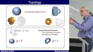
About Topology Topology is basically a study of the global property of the object that is conserved under continuous deformation and that is characterized by some invariants, for example, a ball isdifferent from a donut and you cannot transform a ball into a donut and so on in two dimensions. surface this is usually characterized by an integer so topology is a global property and on the other hand geometric properties are like curvature our local properties but the integral over the local properties can often characterize the topology global of an object, so a famous example would be the Gauss opens a theorem applied to a 2d surface if integrated over the Gaussian curvature of a compact to the surface, it would always be equal to 4pi times 1 minus an integer, so for the sphere that integer number would be 0 for the donut it would be 1 and Now, if we look at the electronic structure of a material, it turns out that the topology of the electronic state in the Breann zone, which is a compact object that I mentioned at the beginning , the local geometry row, is actually taken by a quantity that we call The Barry connection is defined for this relation where u is just the periodic part of the box or wave function, so in fact the study of The non-tropic topology of the black bands of the boat in recent decades will lead to a much deeper understanding of a number of physical phenomena, including protected limit states, the entire quantum Hall effect and new phases of matter, from In fact, two years ago the Nobel Prize was awarded on this topic, what we have discovered is to observe these biological phases of the 1d crystal. that the topological phases of 1d crystals can be characterized by observing the various phases that integrate into the Brillion zone and the Breann zone for a 1d system or ribbon, it is like a circle, so it can be characterized by a number, that number is 0 or 1 we call that number Z 2 and what we have discovered is that all graphene nanoribbons with a certain spatial symmetry have topological phases protected by symmetry and that due to the BOC binary they correspond to the one that is well developed in the field of topological phases of materials. will lead to very interesting final and limit states between segments with different topologies, so our main finding for these graphene nanoribbons is the following: they are materials with a large gap with non-trivial topological phases, those topological phases are protected by symmetry and other It is very interesting about graphene nanoribbons that this topological invariant can actually change with different terminations and afterribbons and that will have important physical consequences.
In fact, you could say that for armchair graphene nanoribbons you could fully characterize and find out what this c2 invariance is. Depending on what type of end the tape has and how many layers or carbon atoms the tape forms, I won't go into the details here, but some important consequences follow: Suppose I look at a joint between two such tapes, say a tape with nine rows of common atoms, a tape with seven rolls of common atoms, if you put them together this way, hence the interface, then you can work. Find out what it says e2 is for this side and that side in this geometry.
See that Z 2 is equal to 1 on both sides, so they are topologically in the same equivalent and the d-r-e said that there should be no interface state, on the other hand, if I take this segment on the right and move up a roll and join them symmetrically like this, then z2 on the left in the chat does not change is equal to one, but on the right is equal to zero and that so that you have a union of topologically invariant objects and that should give you an interface state , a topologically protected interface state, in fact this is a graph of said calculator interface state and this should have some interesting physics associated with it.
I'll come back to that later, what if I look? a single insulator with tape, so if you look at the end, then the junction between the vacuum and the tape that has the vacuum is a trivial topological phase, z2 is equal to zero, but inside z2 it is actually equal to one, so what you hope this is an end to. indicate here and in fact if you look at the literature you will find that people have actually seen these final states, there are some STM images of the end of exactly this seven Amtrak graphene nanoribbon, so you will see that this is the final state and this is NC state.
Although people have not interpreted it in terms of these types of topological phases, one could also change the topology of the electronic state by introducing dopants. Here is a pristine graphene nanoribbon junction and this is one with the timer. An adult case of boron dime. That is the case. which actually people already saw this before and because the dopants introduced bad bands into the system, it actually changes the invariance that they make to zero and that gives rise to the interface state and this interface state again is topologically oriented , so it's protected and you happen to have such a periodic junction, then the interface state would be robust spin centers, they're a pair of antiferromagnetic Li, so that's very interesting because now you could make a superlattice of this, then you would have a quantum spin half chain with almost stable tunable coupling chains along with the Alice exponent, we are actually trying to build such a super lattice at this point, we are trying to make a seven nine periodic array of said super network, so as I mentioned four seven nine The union of this symmetric geometry would be an interface state, so it brings them together to form a super network.
So you should expect to have an interface state here in the face state. The ninth tape actually has a smaller gap than a seventh tape, so the interface state is actually broken down more on the knife tape, so if you look at the super network that way, you'll see that the interface states should interact there and they were intact and they were stronger here than through this ribbon, so let me take you this as an interaction which is t1. this interaction is t2, then the binding states would be expected to be topologically shielded and can form two bands within the bandgap of the ribbon.
In fact, that is what you see in theory, the calculation is done. This would be the space between the balls and these two bands. they come from the topology states and in terms of the coupling strength it can be calculated that the energy dispersion should look like this. That's a detail, but the important thing is to know that the energy position and dispersion depend on the coupling voltage. t1 and t2, that means you now have a very stable system where you could change the bandgap and the bandwidth or these topological states just by changing the length of the segment and you would expect the system to be magnetic if the so-called energy e.g.
The Coulomb energy, which is the energy to put an extra electron into this state, must be greater than the gap, so you would expect that this system, right?, would be a magnetic system and, in fact, our colleague in Berkeley, Philip Fisher and micro. I have made tapes. This is an STM image of said tape. You see you have the seven segments here and the nine segments there and they had done the STS scanning tunneling spectroscopy measurement of the electron density states and this is theoretical. prediction these are the two topological bands and these are the images of those states and here are the fusion data.
It has very good agreement both in terms of the accuracy of the state and the character of the states and this result just came out two weeks ago. As you already knew now let me talk about something else related to prohibition topology. This is another thing we discovered recently. What we find is that non-trivial band topology in a two-dimensional system can dramatically change the optical selection rules in photographic physics. of 2D material, so let me start with what is the conventional optical selection rule for the exciting output and you can look it up in a semiconductor book or the standard solid state book, what you will find is that in case of typos, Systems such as gallium arsenide are allowed. so the optically active output ones are like s and by title prohibited some again that put doctors like cuprous oxide then the optically active optical excitonic states are P light and that has something to do with, like in atomic physics, Delta L it has to be equal to one, but what we found is that that is not true in crystals because of a topological effect.
I will try to illustrate this with the case of the electronic property of few-layer graphene. Graphene has no gaps, but if you put it on top of boron nitride, breaking the symmetry of the two sublattices or graphene again, this is a detail, but it gives a gap for the states in the corner of the Breann zone to bilayer graphene, if you apply some electrics to it, it could also open a gap, in fact, that gap depends on the tension of the electric field perpendicular to the layer, so it actually has an adjustable gap in that same with three-layer graphene layers;
However, the states near the band edges for this system are in fact multicomponent states that are composed of many atomic orbitals, so you calculate those wave functions, the components like a component of a roulette wheel, so what you see is that the spinner would actually be around the top of the valence band and at the bottom of the conduction band, it is this winding of the wave function that is going to lead to a non-zero winding number or topological invariants that would change the optical material selection rule, so let me illustrate this by stitching together new torque equations.
The optical transition to exit can be written this way where this coefficient is simply related to the exit in the wave function and then this element of the matrix is the elements of the transition matrix between bands and you could think of it in terms of putting a circularly polarized light to the right or to the left, then this element of the matrix is just complex numbers in two dimensions, now complex numbers. in two dimensions, you might think that it has an amplitude and a phase, so Israel Ector the forms of the vector field when you have a few vectors in two dimensions, you might have the possibility that actually this field has a critical point and has a winding number associated with and that is related to the so-called Pend Oreille critical points and indices in differential geometry and it is this winding number that will go into the selection rule.
What we have shown is that, instead of the O selection rules, the new selection rules for 2D semiconductors is that the optical transition voltage would be zero and the quantum number associated with the angular momentum of the output is equal to minus times the winding number of the dipole matrix element, so if I go back to my free example of bilayer graphene monolayer graphene and Charlie a graphene what you see is that this price right circular and left circular the transition matrix elements in fact they can have a winding number, you go to two minus two one or two, which means that although graphene is the oldest system that our type will allow Interband transition systems, these new selection rules say that from monolayer graphene boron nitride as outputs are active, but for bilayer graphene in the electric field the P outputs are active and an S is very weak and then for three-layer graphene, it is actually the p and d outputs active, so what you actually do the whole calculation using many body theory from the start, then what you get is a result like this which is completely in accordance with this analytical conceptual analysis and what's even more interesting is that, for example, for the case of bilayer graphene. you excite the electron with the exit in the right circular light, the prediction is that the luminescent would actually give you left light or ice unless, unlike the case of conventional semiconductors and this prediction of having pea-bright exit times and a very weak output, have In fact, it has been experimentally confirmed that we did some work to gallop from poor McEwan's group at Cornell or what they did was observe photocurrent measurements in bilayer graphene with different magnitudes of the applied electric field, so It is seen that this is for small and medium fields.
I feel and feel what it is like to choose a cross in a to separate px and a corresponds to the output 1s, so the s states are very weak. We jumped, we were very weakly active, but P states are very, very optically active and this. is our complete calculation, so there is actually very good quantitative agreement between theory and experiment, so this is very exciting because now you have a very strong tunable optical resonance with high quality factors and that could lead to possible applications in terms of tunable infrared detectors like mitting dial and laser and so on, so my collaborators are very excited about these possibilities, let me skip this because it's kind of, but let me say one thing: a lot can be learned about the physical system by looking at mathematics, it turns out that there are many results of differential topology on manifoldstwo-dimensional and for example this dessert theorem called Punk or 1/2 theorem which says the sum of the pangkor index of a compact sugiko object to the features called orioles, so those indices are just the winding number I'm talking about and because the two-dimensional Breann zone is a torus torus, the annika characteristic is a singular zero, which means that the sum of the number of windings has to be equal to zero, which means that if you have a valley semiconductor winding number one has the winding number of Gilda, the opposite so-and-so, that is why graphene systems and two-dimensional transition metals like Caucasian eyes must have the vote that the Valley winding number K is equal to the opposite of the K Prime Molly and look for these kinds of topological effects once you really look at Molly and the multi-valley semiconductors because if you only have one semiconductor, you only have one gap, then the complaining numbers, but if according to this theorem it has than be equal to zero now I think I'm running out of time, so let me mention one more thing and then I'll leave this: the magnetism of magnetars to demand an atomic sheet in a quasi-2D system.
So far we will see optics and electronics, what about magnetism? Can we figure out what it is? Physics is in voting and chemistry and can we control it? In collaboration with my colleagues at Berkeley and also with Vine and Princeton, we have looked at this particular chromium-germanium-Terry terrarium system, which is a ferromagnet in the book, and we want to see if the magnetism persists down to a few monolayers. Some layers. Now there is a very favorite. Because it's interesting? This is interesting because it is a theorem called a mummy. Mermin Wagner's theorem. We claim that there is no ferromagnetism or antifeminist magnetism in one or two-dimensional material in which the spins or magnetic moments are intact quickly and the physical reason for this is because the thermal fluctuation is in the hand, the fluctuations are in the hand and are of low dimension that would destroy the magnetic order at any temperature and to have magnetism. you have to have some kind of anisotropy in the interaction, so what we find is basically the following: I'm going to skip the details and just then calculate the transition temperature based on the layer versus the experiment, I'll just measure the transition temperature using a scanning magnet. -Kerr optical microscopy, so what you see is that the transition temperature actually decreased quite a bit with the decrease in the number of layers that are related to this fluctuation that I talked about and it still exists up to one layer in theory and our calculation exists . in two layers in the experiment we couldn't get to one layer because for some reason it just disintegrates after a few minutes when they try to make a monitor, yes so long range order does exist so there are some in our graphs. be in the interaction and we know where they come from from our calculations, what we really discovered that excited us is that the capacity of this transition temperature is really large when we apply the similar magnetic field of the system, the reason for this is that the The transition temperature for the magnetic transition in three dimensions is basically dictated by the exchange interaction between the spins and is normally very large, on the order of a few hundred Tesla, but magnetism in two dimensions, as I mentioned, comes from the anisotropy and on site and I thought about Usually they come from the spin orbit interaction which tends to be small, so it is on the order of a fraction of a Tesla, so by applying a small magnetic field to the system its nice atrophy could be improved and that's what we found, if you do the calculation and do the experiment then what you find is a farlan, let's focus on this six layer sample, what you see is that you put a fraction of a magnetic field of Tesla, you could actually increase the transition temperature by orders of magnitude and then and this is our theoretical calculation so this is again very exciting because now you have an external knob to turn to change the magnetism in your material so I think I'm running out of time so I'm going to spit, skip the last topic you're interested in, could you ask me about it, basically what we stitched together here is a very strange electron transport property in graphene, you put a random potential , you actually have a super collimation phenomenon, that is, an electron wave packet.
They don't extend, but actually maintain exactly the same shape, but are guided by the fluctuating potential, but I won't have time to talk about this, so let me summarize the talk with some mattresses to take home. I hope I have convinced you that Christel is too atomic thin. different and are potentially very useful, have novel properties that can be tuned by their substrate and activation enhances electron-electron interaction, for example, environmental sensing is central and graphene nanoribbons in particular, 1d topological have topological phases that can be manipulated for science and technology. There are new optical selection rules in 2D, particularly for systems with topological bands, intrinsic magnetism exists down to a monolayer and are highly tunable, and of course there are many other interesting sciences and applications that do not apply to the material that I don't have.
It's time to touch on the topic, so it's the last slide, let me just acknowledge all my collaborators for the work that I did, so all of you were done by my outstanding students and postdocs at Berkeley and these are my main collaborators, or you can expand on this and I would like to thank you for your attention, thank you very much for this description of these intriguing phenomena that you will find in 2D materials. I think we have time for a couple of questions. If you have some, I think this is a throwable mic. some of the technological possibilities in this where some of the ones you know, the first ones you imagine will actually be used, I think in terms of after your atronics, they could be very interesting applications because of the strong excitonic effects. and circular dichroism effects that could be used now, just like graphene, people could think of all kinds of possible applications, but actually getting to the industry is a pretty difficult question.
Hey, can you hear me? Yeah, so I have a question about these topological effects. protected space in graphene ribbons, so I'm not a topology expert. I was wondering these dates that are topologically protected, do you just find them by normal type binding or deep water calculations and the topology framework just provides some sort of new insight or are they completely new by including some topologically inside them? If you do a forced halation it will always appear yes, so topological analysis will give you a new idea of where they came from and you will know that they are protected by adding atoms to them or changing things. a little bit shouldn't destroy those states, so this is like any quantity in topology, the fact that you find it means it stays there no matter how you distort it, warp it a little, thanks questions, what's not up there, yeah, okay, the hand disappeared.
Again, okay, but no more questions, okay, then I guess we'll do it. If that? Yes. I have a comment because you are not at the lower end of your conference. At the beginning you told us about Multi Enmund disulfide. Yes, it has. a large reasoning effect, for example, in pole series pairing, the increasing effect is absolutely large in its two-dimensional right, so the layers interact very, very weakly or maybe you have explained what the effect is. I see a kind of. I have to think about it. When I see one type of explanation, well, I think the explanation is that each layer forms a kind of closed electronic and closed house system and then the two intact layers where we are, so it takes a slide very easily from a Johanna, okay , it's just that. yes, okay, no thanks, okay, if there are no more questions, let's thank Stephen, thank you.
If you have any copyright issue, please Contact