I Can Die Now. - Intel Fab Tour!
May 31, 2024- I have spent most of my career trying to get into a chip factory. Samsung is a big no, Global Foundries was open to it in person, then cheated on me when I followed up and Intel told me no, every time I asked except one. Honestly, I'm pretty overwhelmed today because I'm going to cross three big items off my wish list. I am visiting Israel for the first time, I will delve into the heart of Intel's state-of-the-art Factory 28 and I will be able to tell you about our sponsor. - Zoho CRM, Zoho CRM is a 360-degree solution that offers an intuitive user interface, AI predictions, and a design studio to help you make your sales faster.

Get 50% off with code ZCRM50 using the link below. (upbeat music) (upbeat music) - My
tour
guide today couldn't be more experienced. Dani is Co-GM of Global Semiconductor Manufacturing and started at Intel working in fab 8 in Jerusalem when the latest technology was the Pentium. Microprocessor manufacturing experts can safely skip a couple of minutes, but for everyone else, let's go over the basics. Every CPU dies, each one starting with a cut silicon ingot like the one here. They are surprisingly pure and are exactly 300 millimeters in diameter. If they were smaller, they would increase waste at the edges. I mean, look at this, obviously this is not going to be a working chip if it is cut along the edge of the circle.
More Interesting Facts About,
i can die now intel fab tour...
By the way, a fun fact is that the reason they run the non-working edge through all the same manufacturing processes is that it actually improves the uniformity of the complete chips next to them. Consistency is key in CPU manufacturing, because although we talk about these chips in terms like 14 or 10 nanometers, the components that make up these transistors are much smaller, on the order of less than a nanometer and a small error or contaminant in either of the hundreds of manufacturing steps means that when it dies, it doesn't work. I mean it's a modern miracle that any of this is possible and it's basically unheard of to get an entire 300 millimeter wafer through the fab without a single defective dye.

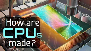
However, before it can be sold, it needs to be transformed from molten sand like this into the brain of your PC. The silicon you see is neither an insulator nor a true conductor. So to create all the little transistors or switches that control current flow through the logic gates and other microstructures of the chip, the wafer needs to go through many processes. The implantation shoots dopant ions at the surface of the silicon to alter its electrical characteristics. So depending on what types of ions are implanted, say phosphorus or boron, you may be laying the groundwork for an n-type or p-type transistor.

This determines whether the voltage is negative or positive to open the door. Diffusion ovens create new blended materials by exposing the wafer to various gases at up to hundreds of degrees Celsius. Lithography is one of the easiest steps to understand conceptually, but also one of the most important. Inside a single processor, there are billions of transistors and literally miles of tiny wires, but they are obviously too small to build and solder by hand. The wafer is then coated with a material called a photoresist and then exposed to ultraviolet light through a mask. Anywhere light passes through the mask, the photoresist will be removed, allowing the exposed parts to be processed.
Then you literally rinse and repeat. Nikon, which by the way does much more than just make cameras, has a great diagram on its site that demonstrates this. So one of those possible processing steps is etching, which aims to selectively remove material from the top of the wafer, creating trenches in it. These can be overfilled with copper to create interconnections and then the excess is removed by polishing with brushes and grout in a process called Chemical Mechanical Planarization. There are different types of engraving, but we can talk more about that once we get into it. (upbeat music) This is it.
Point of no return, here we go. There is no card or anything, yes, it is very, very good, high security. It's time to learn the procedure. This is great, it's very inclusive, they have children's size gloves for people like me. This is crazy. So these are not the gloves that we use in the clean room, these are the gloves to put on the things that we will use in the clean room that will be contaminated and that we will then get rid of. Wow, man, I look good. Now it's time for the second stage. Basically, we have a couple of little foot cover ornaments here and this room is pressurized and the idea is that these are not filtered like the clean room or anything like that, but by having a little bit of pressure in this room, we keep it out. the super stinky air outside.
So when you walk in here, you feel a rush of air coming out and then what you're supposed to do is have dirty things on this side and then clean things on this side. So I have to put on my little boots, did I do it right? Yeah. Okay, so there's more positive pressure here blowing that way, right? - Yes. - So the idea is that the air becomes cleaner and cleaner as we go. Well, what do I do? - You start with the hood. - Yes. - Start from the bot, from top to bottom. - From top to bottom. - Yes. - Okay, why do we go from top to bottom?
So that the dust does not fall from our upper part to our lower part. - It better fit the bunny outfits. - Ah, I already have it. Because that's how the garments layer. I have a feeling our audio won't be the best ever for this video. Ladies and gentlemen, you're going to have to bear with us because my microphone is already under three layers of cloth. (upbeat music) - We leave the dressing room and enter the fabulous room. - To the fabulous. - And it's already crazy. Can you see these like robots on the tracks here?
Apparently these are taking the foups, and I verify that it is actually what is called F O U P, which is 25 wafers. There are 25 slices of the original silicon ingot. That group we just saw, that little robot on the track had hundreds of processors, but we don't know how many of them are good because they're actually on their way to sorting them, where not only will they determine if they work, but they'll determine how well. So is it an I7 core or an I9 core? Every man wants to live, sounds like a nerdy James Bond movie.
I love it. (upbeat music) Oh my god. This place is much bigger than it initially seemed. How many square feet is this? - Four soccer fields. - So the lithography is there. The diffusion is there. - Diffusion there. - ...the result of diffusion. - And the statement was there? - Dry and wet engraving on the side. - Recording. - And flat. - And plan. So we're going to look at all of that, but there's no particular order to these steps because once a group comes in here, you can see, there's whipping everywhere. There are hundreds of stages.
Each Alder Lake CPU die can go from lithography to brushing to deposition, back and forth hundreds of times (happy music). Each silicon wafer comes to the ground to broadcast and basically what these machines do. They are more like an oven and will take the top layer of silicon from the wafer and diffuse it with some type of other material. I asked for some examples, but other than the silicon oxide, they didn't really say anything and in fact didn't even tell me what the first layer of material would be for the pure processors they are making here now.
Here we go, we can see the robotic arm inside that would take out the silicon wafers from the batter and place them as needed for the machine. This is the loading area down here that we can see through the window and then upstairs is the oven where it gets up to 100 degrees and then it has gases that help them achieve whatever type of chemical changes they're making. for above the wafer. One thing that Intel has been very particular about is not touching anything because it's more than just, you know, not pressing the wrong button, but even just hitting these machines.
When you try to build something that has structures that are on the order of nanometers, that means that the building blocks of that thing are subnanometers in some cases. So you can't actually, you can't crash into one of these machines while it's running, and in fact, they only build their factories in particularly stable parts of the world where they don't have to worry about seismic activity. This is great. As we move forward with the spread, we have a great opportunity to show you the multi-level structure of the factory. So what we are walking on is only 1 of 4 layers in total.
Above us there are filters and the air comes from there to here. Then below us is where they will have pumps, chemical delivery, you can see these holes in the floor here. In fact, you can see that there is like a foam, like a kind of vent that goes up to the machine that is next to us and then the air flows from top to bottom to go down to that layer, then it goes down to one more layer where it has water, utilities such as electricity and exhaust. So that the air goes back up the side of the building and recirculates.
In total, Intel expects between 0 and 1 part particles, what was the unit of volume? 1 cubic meter and, to put it into context, an operating room could have tens of thousands of particles per cubic meter. So you may be able to perform surgery here, assuming you are qualified. I asked about this sign and apparently it's just to make sure that as people pass through this hallway, they don't accidentally smoke someone leaving the grid room. This is one of those secret areas, even here inside the factory, which is already a secret area because it contains some of the most expensive materials that they need for lithography, and it's also one of the most secret.
Now, under normal circumstances, each of these stations would be occupied by someone. In fact, the entire factory runs 4 shifts a day, 24 hours a day, 7 days a week, 364 days a year, and only closes during Yom Kippur. So I didn't ask because I'm afraid to know the answer, but I think it's probably costing Intel a pretty penny to have us here snooping around while they didn't sponsor the video or anything. Let's definitely thank Intel for how much it's costing them to make this video. In that sense, there is something interesting here. These tools may not be as sophisticated as some of the other tools here at the factory - you have your flathead screwdriver - but the process is fascinating because unplugging a machine like this for more than a few minutes at a time is very , very expensive. .
So they run it like it's a Formula One pit crew. They have all their tools, everything is set up, ready to rock. They say, okay, we're turning it off, we're doing maintenance, come on, come on, come on, come on, come on, come on, turn it on again. That's all. Don't worry, I won't press any buttons. This is the emo button, okay? The machine will be very sad if you press it. This machine here is doing dry etching right now. So the foups go off the track and then while they wait you can see that they are actually sitting because they sit far away from the machine and while they are processing they appear right next to it.
Here, and then you can see there's a robotic arm inside, grabbing wafers and shaking them. He just throws it in here for a span of, I don't know, 5 or 10 seconds, boom, it's dry-recorded. Go back to the group and then the whole group will go to the next step for this particular processor. We don't know exactly what it's producing, but everything here is Intel 7, so as far as I know, they are modern CPUs or maybe future CPUs. Not all dryers are identical as you may imagine. For all the different specialized processes that a wafer goes through, there can be different machinery.
So this is another example of a dry etching machine where the wafer actually sits in this chamber here and does whatever it's doing. Now we return to the lithography area again, which is why the lighting in the factory has changed back to yellow and the reason is that they use UV light to expose the wafers. So if they have white light, it could easily contain parts of the spectrum that could accidentally expose the wafer. So, they have to use these carefully controlled light sources that won't cause any damage to the wafer as they're being torn into the dough or going in and out of the machines.
A curious fact is that each of these machines costs on the order of 30 to 40 million dollars and you don't have to be a rocket scientist to realize it or, rather, a chip architect to realize that when you put this in, many of them are packaged. This in an area the size of four football fields, will cost a pretty penny and it is because of those costs that they actually have this whole row of cabinets. I guess you could call it between the east and west side of fabulous. All of this is full of bugs that are waiting to be processed because the second of those machines is available, you want to load it with silicon so you can make more processors.
Now we have run out of another lithographyOnce, we are on the east side of the factory, which is also tremendously huge and the first machine we encounter are deposition machines. So what they do is they take the wafer and they apply an extraordinarily thin layer of something to it, let's say, for example, metal, okay? Then return to the group, return to the rails, and move on to the next step. Did I ever say we were going to see the planners? - - Yes, you did it. - Now depending on the processing stage of the wafer, remember that you have to go back and forth hundreds of times for a single die, you don't necessarily want the straight edges of a dry embossing, you might want this kind of curved shape of an edge wet.
Now the actual exact shape is apparently extremely important and extremely difficult to control because, unlike a dry etching, you can actually hear the sound of the bomb. You hear that right now, so there are actually chemicals pumping inside. Another key consideration if you have such expensive machinery is training. So one of the things Intel wanted to show us is how they're using augmented reality practically right here in the factory for a variety of purposes. So one is due to COVID 19. Obviously some of the staff couldn't be here in person for an extended period of time. So remote assistance allows someone who is here in person to have someone else write on an outline or explain it to them while hovering in front of them.
Pretty cool. It is also used as a training resource for the maintenance of older machines, so you can learn by doing, and they will actually give us a practical demonstration. Hey, here's our, here's our test guinea pig and you got some of my cup, that's unfortunate. Oh that's amazing. Then it shows you all the tools you need. So there's a little instructional video on how to do it. Very cool. Hey, look at me, I'm a fabulous equipment maintenance technician. Unfortunately, the windows on these machines are pretty dark, but we managed to capture one being processed right now, so we have some pictures to show the guys.
Essentially, after the deposition step, you will end up with an inherent unevenness that needs to be polished. In the past, they may have dipped the wafers to polish them, but now it's actually done with a brush that has a paste that Intel says is very proprietary. They didn't even give me any clues as to what is in this liquid polish, but they did tell me that the pressure and movement has to be so precise that they can remove just a few. atoms or molecules at the same time. You could see the way it moved back and forth in the background, as if it were spinning.
Crazy. One thing missing is that I don't see where that tray is that loads all the wafers. Where the hell is he? Haha, do you understand? Because it's a disaster. By the way, something I didn't mention before is that each of the different types of machines actually have a number, but you also have these animals because Intel figured that out, especially in a multi-layer design like the fab 28, to be able to do I'm sure that the maintenance team downstairs is, you know, shutting down the right machine for maintenance upstairs, it's a lot easier to communicate and a lot easier to remember.
Oh, we're working on a giraffe machine or a ladybug machine. Apparently, most of the personnel we saw there, although we are actually maintenance personnel for the machines and the actual control center or brain of the operation, are elsewhere. So now we'll head there. This is the remote operating center, which could be considered the brain of the factory we just saw. So if something goes wrong, it will appear as an error on someone's screen, so it's everyone's job in this room to optimize the overall performance of the factory. So instead of having technicians on the fab floor, moving things, looking at screens and turning dials, everything is done right here to ensure that they are pumping out as many chips as possible because once you invest 30 to 40 million dollars, In times of a machine, however many there were there, (laughs), you want them to go as hard as possible, as often as possible. (upbeat music) Every shift, they have to do two stretching sessions to, you know, minimize the risk of RSI, because they're basically sitting in front of their computers all day, every day, right? (claps) But like the friend who only invited you to dinner because he wanted to show off his new car, Intel had a bit of an agenda for inviting us here and that is to show the huge investment they are making in fab 38.
So all we just did was see is about to double. At this roundabout, see you later in about two weeks. That entire construction site will be state-of-the-art, next-generation manufacturing technology that will actually integrate so closely with the existing fab that you could take a wafer from one, use the equipment on the other, and then ship it back. if you really needed it, although it will be a long distance for the four of you to travel. To give you an idea of how huge this construction project is, Intel built its own concrete production facility in the corner of the lot that you can see in the back.
Unreal. One of the main reasons Intel is building manufacturing capacity so aggressively right now is a new concept called IDM 2.0 where basically instead of just building their own products, they're going to make products for third-party companies. , which, personally, given that I am very excited because we are in the midst of the largest global silicon shortage ever. Unfortunately, there are a couple of steps in the die creation process that we didn't get to see today. Adding the bumps that connect the dye to the package by electroplating, that doesn't happen here and with quality control. Quality control begins with electronic end-of-line testing, which verifies the functionality of dummy debug structures and transistors that are specifically designed to ensure everything went correctly in manufacturing.
Then we proceed to grouping. Which is the process of classifying good dice according to their capabilities. Obviously, the best of the best will become the I9 core, the next best will be the I7 core and so on. Aside from that 12th Gen or Alder Lake core, it's a fairly unique product for Intel with much of the design and manufacturing done here in Israel. Once the wafer is ready, Intel sends it to one of their other facilities to be cut and packaged and to a second validation step called class where they basically burn each chip to ensure that no degradation occurs and that the packaging was done correctly.
This, along with design phase tests that simulate the effects of CPU aging, is where Intel's reputation for build quality comes from. I mean, think about it, when you're troubleshooting a system that won't boot, the CPU is the last thing you'll check because unless you drop it, it'll probably work. Incidentally, packaging will become much more complicated in the coming years as multi-die processors like the upcoming Sapphire Rapids begin to be deployed and the relatively basic packaging facilities of yesteryear are expected to become much more fabulous. as. I mean, a packaging mistake on a $10,000 server CPU is a pretty costly mistake given that everything has to be thrown away at that stage if something goes wrong.
Maybe that should be the next
tour
I request. I'm right? Actually, I'm not going to push my luck just yet. This was a once in a lifetime opportunity and I am extremely grateful to Dani and his team. By the way, shout out to Karen for having me, to you for coming and sharing it with me and, of course, to my sponsor. Ting mobile. Ting mobile has rates that make it easy to see how much you can save by switching. They have a perfect plan for everyone, no matter what their needs are. Unlimited talk and text for $10, data plans starting at $15, then there's their fixed plan 12 with 12 gigs of data for $35 and unlimited data for $45.If you like the old pay-as-you-go plans, Ting Mobile's flexible plans that charge just $5 per gigabyte are still there. Data can also be shared if you have a family plan, so connect more phones to save more. You'll continue to receive nationwide coverage and award-winning support. In fact, consumer reports named Ting Mobile as their number one carrier in the United States. Virtually any phone will work with Ting mobile, so visit them at linus.ting.com and receive a $25 credit. If you enjoyed this video, maybe check out one of the previous tours. It's been a while, but they are excellent videos.
If you have any copyright issue, please Contact