The World Of Microscopic Machines
Jun 05, 2021Virtually every vehicle made in the last 20 years contains an astonishing piece of technology that lies dormant, sometimes unnoticed for years, until the unthinkable happens: When an airbag deploys, the electronics in the airbag system They take only 15 milliseconds to decide if the forces on the vehicle are correct. sufficiently severe within 60 milliseconds from the moment of impact, the airbag fully deploys. The entire process from initial deployment to vehicle contact occurs at twice the speed of the blink of an eye and at the heart of an airbag system is the same technology that allows our smartphones to detect motion. , inkjet printers for printing, and projectors for projecting an image on a screen, all of these technologies depend on the emerging field of microelectromechanical systems.

Microelectromechanical systems or MEMS are small integrated devices that combine mechanical and electrical components with traditional manufacturing techniques such as milling and turning. and molding become impractical at small scales, so MEMS devices are manufactured using the same batch processing techniques used to manufacture integrated circuits. These devices can range in size from a few microns to several millimeters. What makes MEMS devices so powerful is their ability to sense control and take action. on a
microscopic
scale but generate effects on a macroscopic scale MEMS technologies are highly interdisciplinary in nature and require engineering and manufacturing expertise from a wide range of technical areas, such as integrated circuit manufacturing technology, mechanical, electrical, chemical and fluid engineering, as well as materials science, optics and instrumentation, its applications span several industries, all of which are manufactured at low cost and in large commercial volumes.
More Interesting Facts About,
the world of microscopic machines...
Because MEMS devices are a hybrid of mechanical and electronic mechanisms, they are typically manufactured using a combination of traditional integrated circuit technologies and more sophisticated methods that manipulate both silicon. and other substrates in a material that exploits its mechanical properties in the traditional manufacturing of integrated circuits known as photolithography. A wafer is first coated with a silicon substrate and its surface is oxidized. The surface of the oxide is then coated with a UV-sensitive polymer called photoresist. A pattern. An amount of ultraviolet light is projected onto the photoresist, which is then chemically developed into a mask on the surface during mask development.

The most common positive photoresist can be removed by the developing agent when protected from ultraviolet light, while a negative resist can be removed in areas exposed to UV rays. Light atoms are irradiated onto the exposed regions, penetrating the silicon below in a highly controlled manner, changing its conductive properties, the unmasked oxide layer is chemically removed and the remaining photoresist is chemically washed away and this process is repeated. dozens of times using the remaining oxide layers as a mask for each subsequent layer the accumulation of layers of material with different semiconductor properties form the circuit of the chip in addition to its electrical properties silicon has excellent mechanical properties since it forms the same type of crystalline structure than diamond, although much weaker and harder than most metals.

It is also surprisingly resistant to mechanical stress. It has a higher yield strength than steel in both tension and compression. MEMS manufacturing, much like integrated circuit manufacturing, involves the addition or subtraction of two-dimensional layers on a substrate based on photolithography and etching. The 3D components of MEMS devices are due to the patterning and interconnection of 2D layers stacked together. The manufacturing process of these devices is divided into three general classifications: bulk micromachining, surface micromachining, and high aspect ratio micromachining or damage in bulk micromachining, the substrate is removed in a manner similar to traditional manufacturing techniques. integrated circuit, an oxide mask is created and the exposed substrate is removed.
The itch pattern is determined by the type of etchant. The isotropic etchant removes material equally in all directions, while the anisotropic etchant is limited by the geometry of the structure. For engraving the anisotropic engraver generally engraves faster in a preferred direction. The etch resistance of the substrate can also be controlled by selectively bombarding it with boron atoms in intermediate steps using traditional photolithography techniques, while traditional wet chemical etching can be used as a more common approach. is the use of a reactive gas driven to a plasma state through radio frequency energy in an etching process known as reactive ion etching surface micromachining.
In comparison, it is predominantly additive in nature and is used to create more complex MEMS-based machinery. The material is deposited on the surface of the substrate in layers of thin films, these layers can be structural or an oxide-based scaffold known as a sacrificial layer, then the scaffold is etched leaving only the structural layers. Surface micromachining can create very complex structures with protrusions. Can be used to create slip. Free-moving mechanical structures, actuators and gears, even
microscopic
motors, have been achieved using improved variants of the process to form larger and more complex MEMS structures. Micromachined silicon wafers can be bonded to other materials in a process known as fusion bonding.It is a technique that allows the perfect integration of multiple layers through atomic bonds between them. Fusion bonding allows the use of more exotic materials such as metals, glass, ceramics and even organic compounds such as polymers, enzymes, antibodies and DNA. My look at micromachining differs dramatically from the other two techniques in that it is reminiscent of traditional casting; typically, a metal base is first coated with a thick layer of acrylic, then, through a mask, rays are projected X On the surface creating a shaped cavity, then a galvanoplasty is performed to fill the cavity with metal and finally the acrylic is recorded, leaving the high -appearance micromechanized of a relief metal structure is one of the most attractive technologies to replicate microstructures and high performance and cost-effectiveness of some common products.
Micro
machines
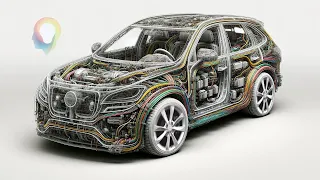
with this technique include fluidic structures such as nozzle plates for inkjet printing and microchannel plates for disposable printing. microtiter plates used in medical diagnostic applications, let's take a look at the popular MEMS device applications we mentioned above and explore how they work. Accelerometers used in automobile airbag sensors were one of the first commercial devices to use MEMS technology and measure rapid deceleration. of a vehicle hitting an object by detecting a change in voltage based on the speed of this voltage change, the integrated circuit subsequently sends a signal to activate the explosive charge of the airbags, the accelerometer mechanism is composed of a capacitive finger structure consisting of a joint pendulum forming the test mass this compliance structure deflects under acceleration or deceleration this deflection creates a differential capacitance the resulting voltage signal created by this is then processed by the circuit in the device initially The airbag technology used a conventional ball and tube type mechanical device that was relatively complex weighed several pounds and cost several hundred dollars The move to MEMS based sensors was directly responsible for the success of MEMS technology and the technology of micromachining in the industry with more than half of these devices operating in vehicles today the reliability of the technology has increased Some vehicles have even been shown to employ dozens of MEMS accelerometers for their traction control, braking and roll assist driving.MEMS-based accelerometers can even be configured to detect motion in three axes. With the rise of smartphones, this capability quickly became indispensable. In this setup, the test mass is suspended in the center of a frame by microscopic springs in a manner similar to a trampoline. Acceleration in the XY plane is sensed by capacitive fingers attached to the frame of each respective axis similarly to a single-axis accelerometer sensor. Both sensing structures also contain electrodes that can sense the vertical. path of the test mass that forms the simultaneous action of a z-axis accelerometer. Accelerometers are not just limited to automotive and mobile phone applications, they can also be found in earthquake detection equipment, virtual reality gaming systems, pacemakers, high-performance disk drives, and even weaponry systems in most of smartphones.
MEMS-based gyroscopes complement the accelerometer, also found in navigation equipment, avionics, and virtually any modern device that requires rotation detection. MEMS gyroscopes work by suspending an accelerometer on a platform which itself uses a MEMS-based solenoid to create a constant oscillating motion. The setup exploits the Coriolis effect in which an angular force applied to a moving mass creates a perpendicular force. The perpendicular force is detected by the suspended accelerometer and then translated to a rotational measurement using the integrated signal processing circuitry, another hugely successful application of MEMS technology. is the inkjet printer head, inkjet printers use a series of nozzles to support ink droplets directly onto a medium, depending on the type of inkjet printer, two popular MEMS technologies are used to achieve This, MEMS-based, thermal and piezoelectric thermal inkjet printer head technology, was invented by Hubert Packard in 1979, the technique uses the thermal expansion of ink vapor to eject ink into the printer head.
There are a number of small resistive heaters. These resistors are activated by a processor in short pulses of just a few microseconds inked on contact. With the resistance it heats rapidly at a speed of one hundred degrees per microsecond, vaporizing the ink to form a bubble. This process is called bubble nucleation. As the bubble expands, a droplet forms and is pushed out of the nozzle, lands on the paper and solidifies. When the bubble collapses, a vacuum is created that draws more ink into the print head from the reservoir. cartridge, sometimes called the bubble jet process. Thermal inkjet printer heads demonstrate that not all MEMS devices require moving parts to operate in a piezoelectric printer head more directly.
A kinetic approach is used. A piezoelectric crystal is located at the back of a chamber in each nozzle. The piezoelectric crystal element receives a very small electrical charge which causes it to vibrate when it moves inward, forcing a small amount of ink out of the nozzle as an element. goes back, introduces a little more ink into the chamber to replace the ink that was ejected, even though it was originally developed by Epson. This technique is used by all major printing companies. Advances in MEMS manufacturing techniques have allowed more ink ejection elements to be incorporated into a printer head.
Early printers had only 12 nozzles with a maximum resolution of approximately 92 dots per inch. Today, modern inkjet printers have up to 600 nozzles that can fire a droplet simultaneously, enabling 1200 dots per inch printing, one of the first uses of MEMS devices in the form of large mechanical assemblies in A single array has been for display applications invented by Texas Instruments. Digital micromirror device technology often marketed as digital light processing or DLP can be found in consumer projectors, high-definition projection televisions, and projectors for large spaces, such as digital cinemas, where traditional liquid crystal technology cannot compete. Digital micromirror devices are composed of a series of millions of tiny pixel mirror elements.
Each pixel is made of a multi-layer device consisting of an aluminum mirror mounted on hinges. These pixels rest on a CMOS memory cell changing the value of the memory cell, forcesElectrostatics alter the angle of the mounted mirror generally by plus or minus 10 degrees. These mirrors can be quickly repositioned to reflect light from a powerful lamp or LED, either through the lens or onto a heat sink known as a light discharge because each pixel quickly turns its reflected light on and off through the lens. . The brightness level is controlled by adjusting the ratio between the on and off time.
The color is achieved by mixing red, green and blue light through the device. The two main methods used are a single one. chip or three-chip method in the single chip method a synchronized color wheel is used to project frames of each color in succession producing the illusion of a color image this method generally creates a moving color distortion known as effect Rainbow The three-chip method addresses the problem by splitting light from the projection source into its component colors through a prism, each primary color is processed through its own dedicated chip and the three reflected images are recombined into the lens.
This technique allows us to obtain more precise and robust colors, as well as sharper ones. Digital micromirror imaging devices formed the basis for another emerging application of MEMS technology. Electro-optical optical communications have been the only practical means of addressing network scaling problems created by the tremendous growth of data traffic routing technologies that rely on electronics to function as a switch. These bottlenecks can be eliminated through the use of all-optical networks that offer far superior performance capabilities. MEMS technology has been proven to be an effective tool due to its small size, low cost and low power consumption.
The durability of consumption and high switching density form a perfect solution to the problem of control and switching of optical signals. Devices such as waveguides, optical switches, cross-connects, and multiplexers have been successfully produced by using a mechanism similar to micromirror display devices. be routed from a source signal to hundreds of possible destinations by directing light through a powered microscopic mirror. This concept has reduced once-expensive optical switching components to below the dollar level. One of the most promising applications of MEMS technologies has been the emergence of biomedical MEMS devices, called bio MEMS devices, tend to focus on fluid processing at microscopic scales conceptualized as a lab-on-a-chip.
These devices can incorporate micro
machines
, fluid pumps, chemical sensors, flow controllers, nozzles, and valves into their overall design. This class of devices. enabled rapid, inexpensive, and relatively convenient manipulation and analysis of small volumes of biological fluids. One of the first and simplest examples of a bio MEMS device is the micromachined microtiter plate. A microtiter plate is a flat plate with multiple wells that is used as small test tubes for testing. and analysis MEMS technology has been applied to create microtiter plates with working areas of less than 6 square centimeters. They are formed from plastic with a high aspect ratio of micromachined microchannels.The small sizes of these plates allowed for automatic filling by using capillary action despite the simplicity. Of these initial applications, the future of bioMEMS devices lies in their potential to deliver pharmaceuticals in a highly specific manner. Insulin control. Hormonal therapy. Chemotherapy and pain control can be achieved by carefully releasing drugs into the body from small chambers embedded in a MEMS. device Some advanced bio MEMS research allows detecting the body's own internal chemistry to regulate drug release. Several bio MEMS research laboratories have even demonstrated the capture of a single red blood cell and the subsequent injection of a protein into it through a 5-micron channel.
These techniques open the door to direct cellular manipulation with DNA proteins and pharmaceuticals. The potential for MEMS devices is amazing applications, from ultra-miniature, highly integrated low-loss tracking radio antennas to sensors that can measure heat radiation, light, acoustics, pressure, motion, and even detect chemicals. like MEMS. Technology-based machinery becomes more refined, we are approaching a new frontier of nanotechnology that will revolutionize entire industries by challenging our current ideas about the economics of manufacturing.
If you have any copyright issue, please Contact